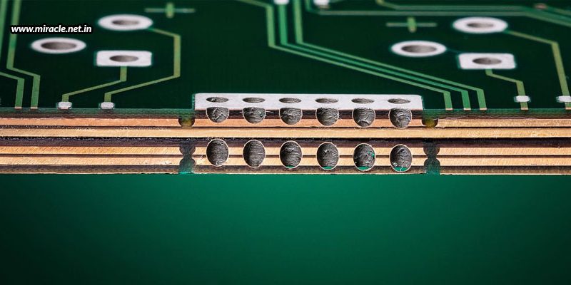
What Is Heavy Copper PCB Or Thick Copper PCB?
In some real-life high-power applications, ultra-high thermal management compatible with high-power currents is required. Thick copper PCBs are especially good at managing current flow and dealing with special situations. Typically, standard PCBs have copper thicknesses in the 1OZ to 3 OZ range. Heavy copper PCB or thick copper PCB is the type of PCB with finished copper weight between 4oz and 10oz. In some super thick copper PCBs, the copper thickness per square foot may reach 20oz to 200oz. These PCBs are used for high current output and thermal management optimization. Thick copper layers allow large PCB cross-sections for high current loads and facilitate heat dissipation. In electronics applications, temperature management is particularly important. Excessive temperature can seriously damage the performance and life of the circuit board. Using this PCB technology, it is also possible to combine finely laid out structures on the outer layers with thick copper layers on the inner layers.
The width, thickness and purity of copper determine the strength of the PCB, which can make an otherwise fragile circuit board harder and more durable. Of course, the thickness and width of the heavy copper PCB need to be determined according to the impedance and compatibility of the project. This kind of PCB is called heavy copper pcb/ thick copper PCB. These PCBs are used for large current outputs and optimization of thermal management. The thick copper allows large PCB-cross-sections for high current loads and encourages heat dissipation. With this PCB technology it is also possible to combine fine layout structures on the outer layers and thick copper layers in the inner layers.
Common heavy copper PCB processes are as follows:
Blue Bar: Insert the thick copper bar into the circuit board. This approach reduces the overall weight of the PCB by saving material. The uniformity of the plane is improved by the resin flowing into the space in the copper circuit.
Laminate deposition: This process uses a thick base copper. This method is relatively consistent and reliable when placing etch. It is convenient to regulate the edge of the trace and provide fine trace and space.
Buried Copper: Insert thick copper into the prepreg in advance. The copper thickness of this method is determined by the resin thickness, using laser cutting.
With the advancement of JHD plating technology, our thick copper plated holes and sidewall copper thickness control have become more and more handy. As a result, impedance control and high-current circuits are integrated to achieve a high-density and more stable circuit structure. We will do custom heavy copper pcb production work according to your project needs.
It is now possible to mix standard circuits with thick copper on a single board to achieve: reduced layer count, area savings, low impedance power distribution and cost savings. Designers need to discuss manufacturing tolerances based on schematics and PCB design drawings to meet project requirements before performing hybrid articulation.
In order to ensure the quality of the PCB board, it is necessary to select a suitable solder mask and control the screen printing process. In respect of electrical performance, the thickness of the solder mask will greatly affect the safety, impedance,and feasibility of PCB assembly, Therefore, the manufacturer must control the thickness of the solder mask strictly.
How To Measure The Thickness Of Solder Mask?
The thickness of the PCB solder mask depends on the material and the type of PCB. In addition, the thickness of the PCB solder mask varies from place to place. The thickness of standard PCB solder mask is 8-15um, and the usual thickness is 10um.
The sprayed solder mask thickness will be slightly thinner, while the curtain covered solder mask thickness will be slightly thicker.


